If your aim is to achieve good grades in Class 12, then NCERT Solutions at Aasoka are the best educational resources one can rely on. The solutions make students understand the concept better hence, in turn, helping them get the scores they desire. The NCERT Solutions for Class 12 is designed by the subject matter experts keeping the latest CBSE syllabus in mind.
“Electronic Devices” of Physics Class 12 includes the following topics: semiconductors and insulators, special purpose p-n junction diodes, solar cells, LED, energy bands in conductors, photodiode, n-type semiconductors, dopants, carriers, and so much more.
Question 1:
14.1. In an n-type silicon, which of the following statement is true ?
- Electrons are majority carriers and trivalent atoms are the dopants.
- Electrons are minority carriers and pentavalent atoms are the dopants.
- Holes are minority carriers and pentavalent atoms are the dopants.
- Holes are majority carriers and trivalent atoms are the dopants.
Answer:
(c)
Question 2:
Which of the statements given in
Exercise 14.1 is true for p-type semiconductors ?
Answer:
(d)
Question 3:
Carbon, silicon and germanium have four valence electrons each. These are characterised by valence and conduction bands separated by energy band gap respectively equal to (Eg )C , (Eg )Si , and (Eg )Ge . Which of the following statments is true ?
Answer:
(c)
Question 4:
In an unbiased p-n junction, holes diffuse from the p-region to n-region because
- free electrons in the n-region attract them
- they move across the junction by the potential difference
- hole concentration in p-region is more as compared to n-region
- All the above.
Answer:
(c)
Question 5:
When a forward bias is applied to a p-n junction, it
- raises the potential barrier
- reduces the majority carrier current to zero
- lowers the potential barrier
- None of the above.
Answer:
(c)
Question 6:
For transistor action, which of the following statements are correct ?
- Base, emitter and collector regions should have similar size and doping concentrations
- The base region must be very thin and lightly doped
- The emitter junction is forward biased and collector junction is reverse biased.
- Both the emitter junction as well as the collector junction are forward biased
Answer:
(b), (c)
Question 7:
For transistor amplifier, the voltage gain.
- remains constant for all frequencies
- is high at high and low frequencies
- is low at high and low frequencies and constant in the middle frequency range
- None of the above.
Answer:
(c)
Question 8:
In half-wave rectification, what is the output frequency if the input frequency is 50 Hz ? What is the output frequency of a full wave rectifier for the same input frequency ?
Answer:
Given input frequency = 50 Hz.
Output frequency
For Half wave rectifier = 50 Hz
For full wave rectifier = 50 × 2
= 100 Hz.
Question 9:
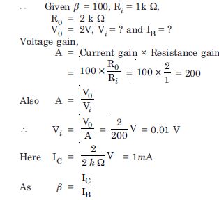
For a C.E. transistor amplifier, the audio signal voltage across the collector resistance of 2k is 2V. Suppose the current amplification factor of the transistor is 100, find the input signal voltage and base current, if the base resistance is 1 k .
Answer:
Question 10:
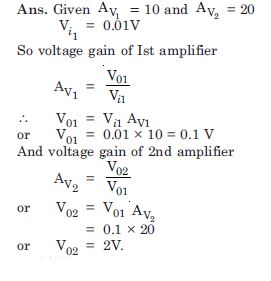
Two amplifiers are connected one after the other in series (cascaded). The first amplifier has a voltage gain of 10 and the second has a voltage gain of 20. If the input signal is 0.01 volt, calculate the output a.c. signal.
Answer:
Question 11:
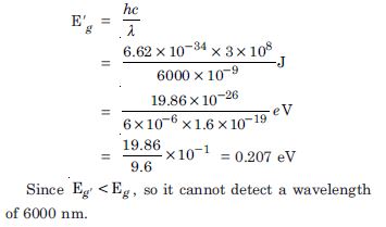
A p-n photodiode is fabricated from a semiconductor with band gap of 2.8 eV. Can it detect a wavelength of 6000 nm ?
Answer:
Band gap Eg = 2.8 eV
Energy band gap corresponding to wavelength 6000 nm is given by


